Research Highlights
"Semiconductors Enter the Era of Skyscrapers": Stacking Chips Like High-Rise Buildings to Boost Performance
- Mechanical Engineering
- Date2026.07.07
- Views179
[POSTECH Demonstrates Stable Stacking of More Than 10 Ultrathin Si Chips,
Achieving Four Times Higher Integration Density Than Commercial HBM]
A Korean research team has developed a technology that enables the stable stacking of more than ten ultrathin semiconductor chips, each only one-fifth the thickness of a human hair. A research team led by Prof. Seok Kim and integrated Ph.D. student Uhyeon Kim from the Department of Mechanical Engineering at POSTECH, together with Dr. Hohyun Keum of the Korea Institute of Industrial Technology, successfully achieved an integration density approximately four times higher than that of commercial high-bandwidth memory (HBM) through a novel process that simultaneously transfers chips and forms metallic interconnections. The study was published in the international multidisciplinary engineering journal Results in Engineering.
AI services such as ChatGPT, image-generation AI, and autonomous vehicles share one common requirement: they must process enormous amounts of data at extremely high speeds. While electronic devices continue to become thinner, semiconductor performance continues to improve because chips are no longer expanded laterally but stacked vertically. This is analogous to constructing high-rise apartment buildings instead of single-family homes when urban land becomes scarce. High-Bandwidth Memory (HBM), a key technology that determines the performance of AI accelerators, is built by vertically stacking multiple memory chips, making the ability to reliably stack a large number of chips a critical challenge.
The difficulty lies in handling ultrathin chips. As chip thickness decreases below several tens of micrometers (μm), becoming thinner than a human hair, chips become increasingly susceptible to bending, warping, and fracture. Much like a stack of thick cardboard remains flat while stacked layers of delicate rice paper easily wrinkle and become misaligned, the challenge becomes more severe as the number of stacked layers increases.
Conventional semiconductor packaging processes primarily rely on flip-chip bonding and carrier-wafer-based grinding processes. However, flip-chip bonding requires highly precise pneumatic nozzle design and process control, while grinding-based approaches often suffer from handling damage and warpage. These issues become significantly more pronounced when chip thickness falls below several tens of micrometers. To address these limitations, the researchers leveraged the inherent stability of transfer printing technology, demonstrating both reliable integration and the fabrication of chips with thicknesses in the 10-micrometer range.
To overcome these challenges, the team combined two technologies into a single process platform: Transfer Printing, which precisely places chips at desired locations, and In-situ Bonding, which forms metallic bonds simultaneously during chip transfer. This integrated approach allows chip transfer, placement, and electrical interconnection to be completed in a single process.
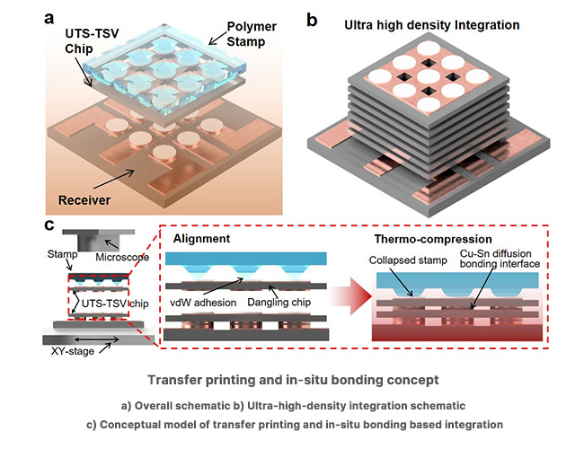
To validate the new process, the researchers fabricated ultrathin silicon chips approximately 14 μm thick. Each chip incorporated both vertical electrical signal pathways and lateral redistribution wiring, making the structure highly suitable for multilayer integration.
Using the developed process, the team successfully stacked more than ten ultrathin chips under low-temperature (below 180°C) and low-pressure (below 20 kPa) conditions. Even after repeated stacking, interlayer alignment errors remained extremely small, and structural warpage was significantly suppressed. The achieved integration density—defined as the number of stacked layers relative to total package thickness—was approximately four times greater than that of conventional 12-layer HBM structures. In other words, substantially more chips can be accommodated within the same vertical height.
Commercialization of this technology could dramatically increase the number of chips integrated within a given space, enabling significant improvements in AI semiconductor performance. Furthermore, the technology has potential applications beyond memory devices, including chiplet-based heterogeneous integration and next-generation micro-LED displays, suggesting a broad technological impact.
Prof. Seok Kim of POSTECH stated, "By we achieved an integration density approximately four times higher than existing HBM technologies, we expect this technology to become a key enabling technology for future high-performance AI semiconductors and next-generation memory systems.“
Dr. Hohyun Keum of KITECH noted, "Micrometer-scale ultra-precise alignment and bonding technologies developed in this work could be widely applied to next-generation semiconductor and display manufacturing.“
This research was supported by the National Research Foundation (NRF) of Korea through the PIM AI Semiconductor Core Technology Development Program (Device) and the Mid-Career Researcher Program.
Researcher
-

Kim Seok Professor
Dept. of Mechanical Eng.
View Profile -
Uhyeon Kim
MS/PhD integrated program


