Research Highlights
A Hidden Phase of In2Se3 Emerges as a Wafer-Scale Logic Semiconductor
- Chemical Engineering
- Date2026.10.02
- Views386
[POSTECH-KAIST Team Demonstrates 4-Inch Wafer-Scale κ-Phase In2Se3 Transistors Fabricated at 250 °C]
Just as carbon atoms arranged in different ways can form either graphite or diamond—the hardest natural material—semiconductor materials can also exhibit completely different properties depending on their atomic arrangements. Now, a previously overlooked crystal structure of indium selenide (In2Se3) has been brought to life as a promising material for next-generation logic electronics.
A research team led by Professor Yong-Young Noh from the Department of Chemical Engineering at POSTECH, including graduate student Jaeyun Lee, in collaboration with Professor Jimin Kwon and Dr. Yongwoo Lee from the School of Electrical Engineering at KAIST, has successfully realized wafer-scale logic transistors based on the rarely explored κ-phase In2Se3. The study has been published in the international journal Nature Communications.
In2Se3 has long been considered a promising next-generation semiconductor material because of its atomically thin structure and excellent charge transport properties. However, previously studied crystal phases have shown limitations. Their ability to retain a previous electrical state after voltage removal—known as a “memory effect”—is beneficial for memory applications, but can cause instability in logic circuits that require identical outputs from identical inputs. In addition, although high performance has been demonstrated in small exfoliated flakes, achieving uniform and high-quality In2Se3 films over large wafer areas has remained a major challenge for practical semiconductor manufacturing.
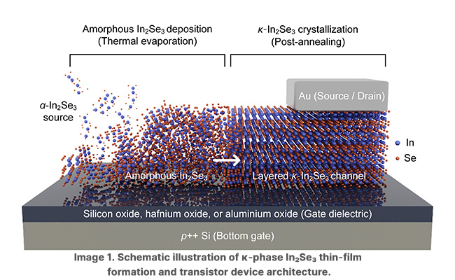
The research team turned their attention to the previously underexplored κ-phase In2Se3. Unlike conventional In2Se3 phases, the unique atomic arrangement of the κ-phase suppresses ferroelectric memory effects, making it more suitable for stable logic operation. Using an industrially compatible thermal evaporation process followed by a low-temperature annealing treatment at 250 °C, the researchers successfully fabricated approximately 10 nm-thick κ-In2Se3 films uniformly across an entire 4-inch wafer. The low processing temperature, below 450 °C, also satisfies the thermal requirements for three-dimensional semiconductor integration, allowing additional electronic layers to be built on top of existing silicon circuits without damaging them.
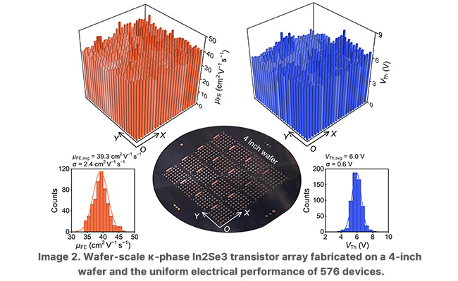
The fabricated devices demonstrated outstanding electrical performance and uniformity. A total of 576 transistors (24 × 24 array) distributed across the wafer exhibited highly consistent characteristics regardless of their position. The devices achieved an average electron mobility of 39.3 cm2V−1s−1 and an on/off current ratio exceeding 108, representing a high level of performance among large-area thin-film two-dimensional semiconductor devices. Furthermore, the transistors maintained stable operation under 10 million repeated switching cycles using ultrashort 100 ns electrical pulses, demonstrating both fast switching capability and long-term operational reliability required for logic applications.
To further demonstrate its potential as a logic semiconductor, the team integrated κ-In2Se3 with a p-type selenium-alloyed tellurium oxide (Se-TeOx) semiconductor featuring complementary charge transport characteristics. By combining n-type κ-In2Se3 and p-type Se-TeOx devices, the researchers successfully implemented a complementary inverter circuit, a fundamental building block of modern logic electronics. This result provides direct evidence that κ-In2Se3 can serve not only as a memory-related material but also as a stable platform for logic semiconductor applications.
This study demonstrates that In2Se3, previously regarded mainly as a memory-oriented material, can be transformed into a wafer-scale logic semiconductor by utilizing an alternative crystal phase with suppressed memory effects. The ability to fabricate uniform large-area films at low temperatures is particularly significant for future three-dimensional integrated electronics, where new semiconductor functions are stacked vertically on existing silicon chips. This work opens a pathway toward smaller, more powerful, and highly integrated semiconductor technologies.
Jaeyun Lee, an integrated M.S./Ph.D. student at POSTECH who led the study, stated, “In2Se3 has mainly been investigated as a ‘memory semiconductor’ due to its intrinsic ferroelectric properties. Our work expands its potential by introducing the less-explored κ-phase as a stable material platform for logic semiconductor applications.”
This research was supported by the Ministry of Science and ICT, the National Research Foundation of Korea, and the Glocal University 30 Project.
Researcher
-

Noh Yong Young Professor
Dept. of Chemical Eng.
View Profile -

Jaeyun Lee
MS/PhD integrated program