Research Highlights
Swapping Atoms to Tailor Semiconductor Materials: A New Route to Next-Generation High-Performance Devices
- Materials Science & Engineering
- Date2026.11.17
- Views53
[POSTECH Professor Moon-Ho Jo's team develops a “modular transistor fabrication technique”
that creates semiconducting, insulating, and semimetallic regions through selective atomic substitution]
Researchers have developed a new technique to precisely engineer two-dimensional (2D) semiconductors, a leading candidate material for next-generation chips, one atomic layer at a time. The technique is expected to simplify complex material-stacking processes and help bring ultra-small, low-power semiconductors closer to reality.
The Ministry of Science and ICT (MSIT) announced that a research team led by Director Moon-Ho Jo of the Center for van der Waals Quantum Solids at the Institute for Basic Science (IBS), who is also a POSTECH Distinguished Professor※, has developed a “modular transistor fabrication technique.” By selectively replacing the atoms that make up a 2D semiconductor, the method creates semiconducting, insulating, and semimetallic regions at any chosen layer and position within a single thin film.
The research was supported by MSIT through its IBS research center program and was published in Science on October 16, 2026, at 3:00 a.m. KST.
As artificial intelligence advances, research to make semiconductors smaller and more power-efficient has intensified. 2D semiconductors, which can control electrical current even at a thickness of a single atomic layer, are drawing attention as a next-generation material that could overcome the scaling limits of conventional silicon. Global chipmakers and research institutes are making progress toward applying them to industrial wafer processes. However, turning them into working electronic devices still requires the precise integration of different materials, which remains a technical challenge.
The transistor, the most fundamental semiconductor device, acts as a switch that turns current on and off. It requires a semiconductor through which current flows, an insulating layer to control that current, and metal electrodes through which current enters and exits. 2D semiconductors, however, do not readily bond chemically with other materials at their surfaces, making it difficult to deposit a uniform insulating layer. Attaching metal electrodes directly can damage the contact interface or increase electrical resistance, degrading performance. Another approach—transferring and stacking different thin materials one sheet at a time—is so complex that it has proven difficult to apply uniformly over large areas or scale up to mass production.
Instead of stacking different materials, the research team devised a way to create the required materials directly at desired locations by selectively replacing the atoms of the 2D semiconductor itself.
The team worked with tungsten diselenide (WSe₂), a p-type semiconductor1) in which a layer of metallic tungsten (W) atoms is sandwiched between layers of selenium (Se) atoms. The researchers took advantage of the principle that leaving the central tungsten atoms intact while replacing only the surrounding selenium atoms with other elements changes the material’s electrical properties.
In multilayer WSe₂ films, the team selectively replaced selenium atoms at targeted layers and positions with oxygen (O), sulfur (S), or tellurium (Te). This converted those regions into insulating tungsten oxide (WOₓ), n-type semiconducting tungsten disulfide (WS₂), and highly conductive semimetallic tungsten ditelluride (WTe₂), respectively.
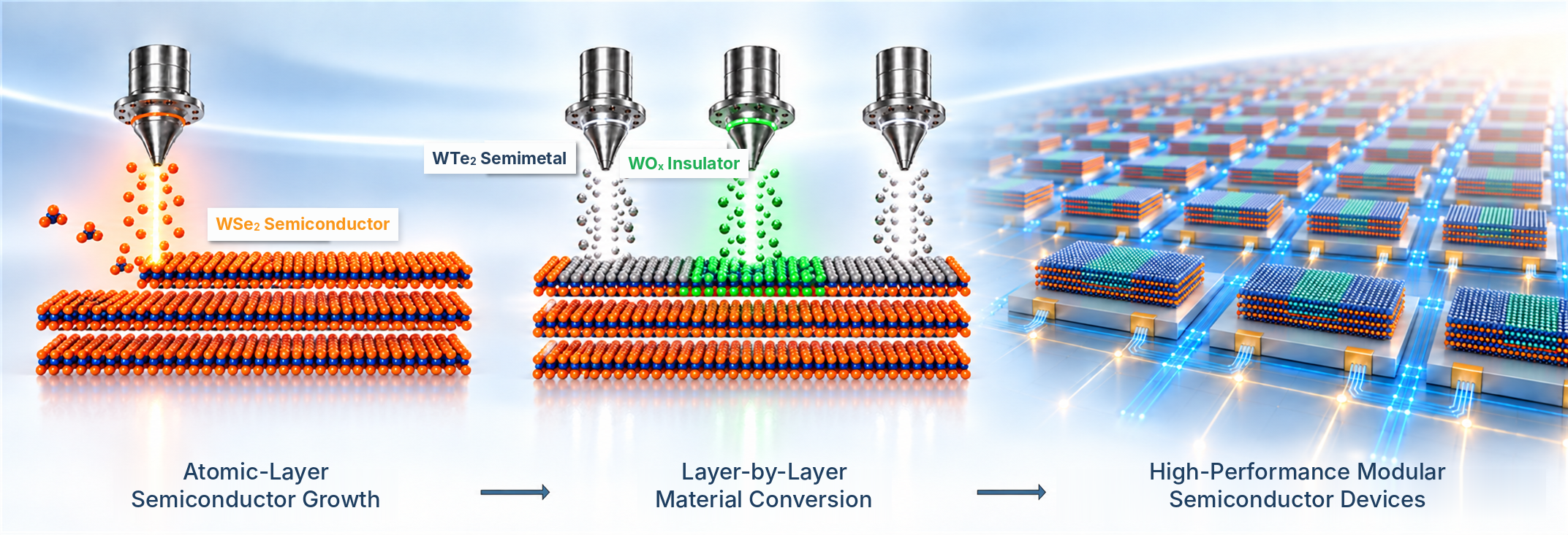
The process exploits the fact that the tiny gaps between the film’s layers act as barriers that block the movement of reactive atoms. By adjusting the reaction temperature and the pressure of the reactant gas to control whether the chemical reaction proceeds into the next layer, the team converted the material one atomic layer—about 0.7 nanometers (nm) thick—at a time. Using masks of the kind employed in semiconductor processing, they also succeeded in converting only selected areas within the plane of the film.
With this technique, the researchers fabricated a modular transistor that integrates a semiconductor (WSe₂), an insulating layer (WOₓ), and a semimetallic electrode contact layer (WTe₂) within a single film. Introducing the semimetallic contact layer, which facilitates current flow, lowered the energy barrier that charges must overcome when moving from the metal electrode into the semiconductor to 35.5 millielectronvolts (meV)—roughly one-third of that for directly attached metal electrodes—allowing current to flow more easily.
The device’s switching performance also approached the theoretical limit. The change in gate voltage required to change the current tenfold was 61.3 millivolts, close to the theoretical minimum of about 60 millivolts achievable by conventional transistors at room temperature. The ratio of on-state to off-state current exceeded 10 million, confirming that current can be stably controlled with only small changes in voltage.
In addition, the WOₓ insulating layer achieved an equivalent oxide thickness (EOT)—a measure that expresses electrical performance in terms of thickness—of less than 1 nm, meeting the key performance target for ultra-scaled devices set by the International Roadmap for Devices and Systems2).
Going further, the team vertically stacked p-type and n-type transistors to build a complementary inverter, a basic building block of digital circuits that reverses an input electrical signal. The inverter successfully inverted signals at a low voltage of 1 volt (V), demonstrating that the technique can be extended beyond individual devices to stacked integrated circuits.
The study stands out for going beyond improving individual materials or interfaces: it realizes the key components of a transistor within a single thin film. The researchers plan to apply the technique to a range of 2D semiconductor materials, develop it into a wafer-scale, large-area process, and explore its potential for next-generation ultra-small, low-power semiconductor technologies such as 3D stacked integrated circuits.
“This study is significant in that it brings atomic-scale material manipulation, a technique from fundamental materials science, into modern semiconductor technology, opening a path toward a qualitative leap in future chip technology,” said Director Moon-Ho Jo. “It can be extended not only to ultra-low-power, ultra-small semiconductors but also to next-generation stacked semiconductor device technologies.”
“This research is a prime example of innovation in which basic science has solved a long-standing challenge in semiconductors, a next-generation national strategic technology, and presented a new process paradigm,” said Kim Sung-soo※, Deputy Minister for R&D Policy※ at MSIT. “We will continue to fully support basic and fundamental research so that core technologies can translate into Korea’s industrial competitiveness.”
▶️ DOI: https://doi.org/10.1126/science.aei2693
1)p-type and n-type semiconductors: A semiconductor is p-type when current is carried by positively charged holes (vacancies left by departing electrons), and n-type when current is carried by negatively charged electrons.
2)International Roadmap for Devices and Systems (IRDS): An international technology outlook that sets out the direction of technological development in the global semiconductor industry, along with the device performance and technology targets required in the future.
Researcher
-

Jo Moon-Ho Professor
Dept. of Materials Science & Eng.
View Profile -

Seok Young Min
Dr.
-

Hyunje Cho
MS/PhD integrated program
Related News
-
New Semiconductor Quantum Materials Developed, Enabling Exceptionally Efficient Light Emission for Future LEDs
2026.04.28 -

Aluminum Prevents 'Rapid Aging' in High-Energy Batteries
2025.12.05 -

Could High-Temperature Single Crystals Enable Electric Vehicles Capable of Traveling Up to One million Kilometers?
2024.07.10